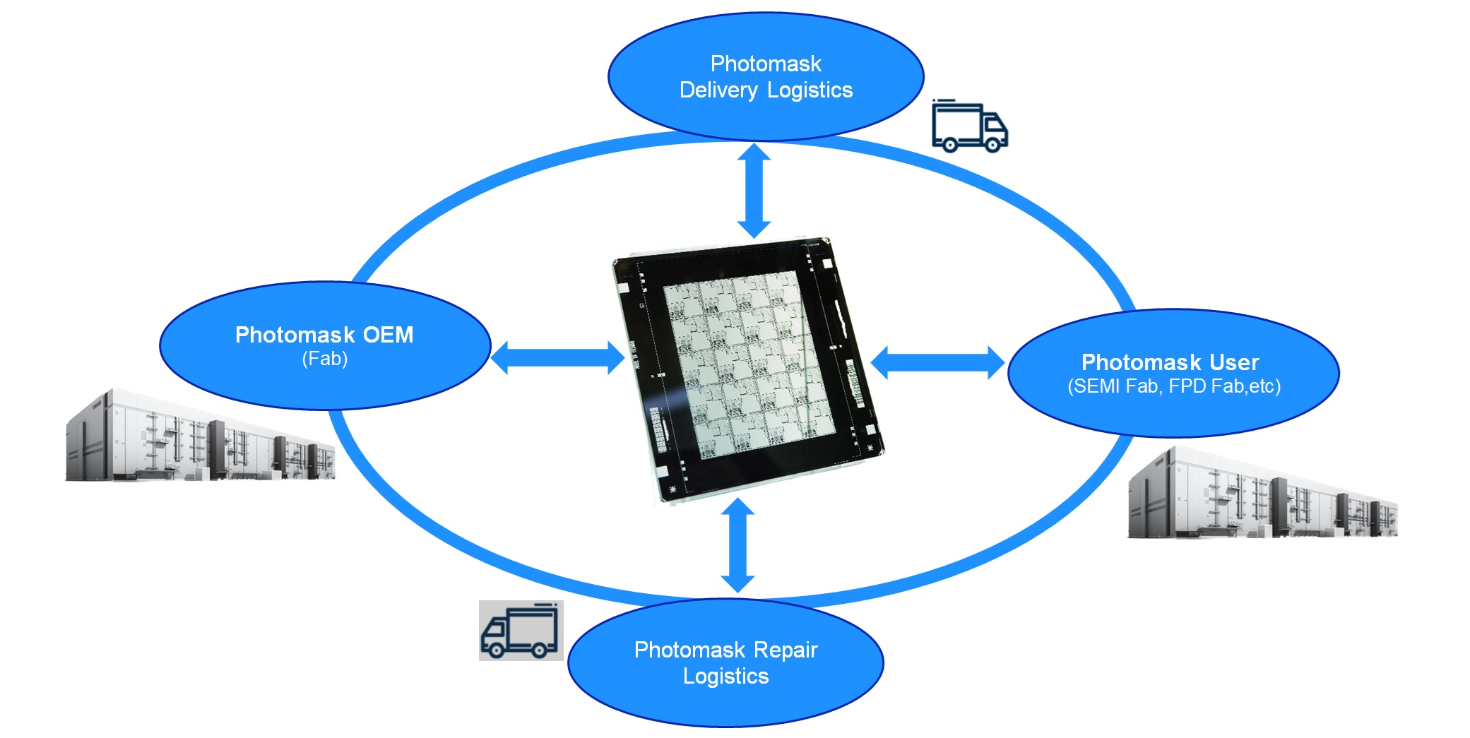
1. Photomask Basics
Photomask, or reticles is the critical tool used in nowadays semiconductor lithography process to form the device patterns on a silicone wafer substrate.
Regarding the electrostatics impacts, photomasks for DUV (Deep Ultra-Violet) lithography technology are mainly involved which includes binary masks and phase shift mask (PSM).
2. Electrostatics Impacts Modes on Photomask
The Electrostatics impact on photomask by the electric field strength, including ESD (Electro-Static Discharge) damage and the other more important EFM (Electric Field induced ion Migration) spreading and protrusions.
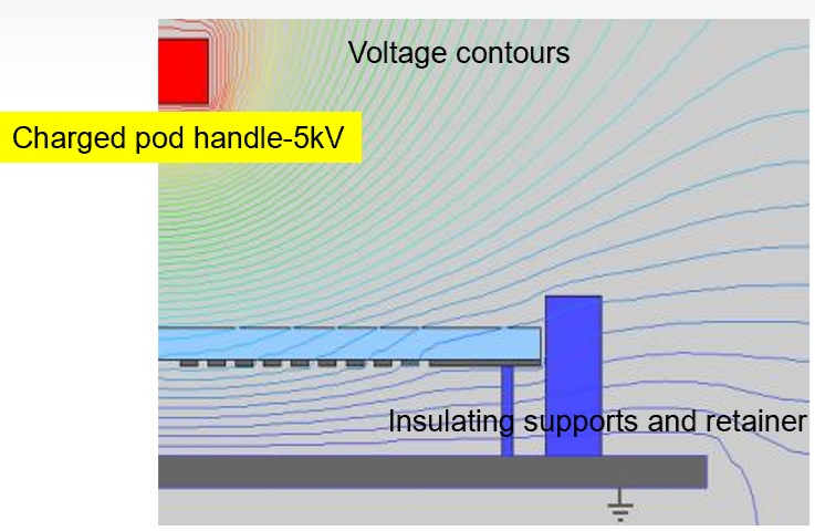
Electrostatic charge source impacts on photomask patterns by electric field strength (Source: Gavin Rider / Microtome Inc.)
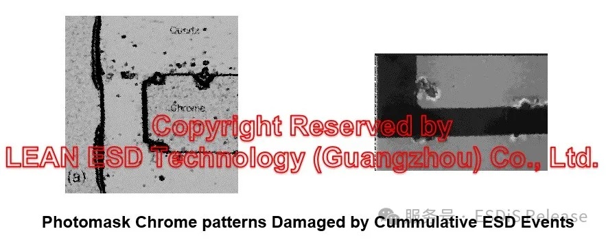
Typical Photomask Chrome pattern damage symptoms caused by ESD events
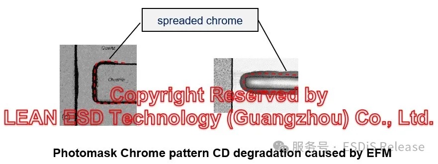
Typical photomask chrome pattern damage symptoms caused by EFM events
3. The Effective Inspections to detect Photomask damages caused by Electrostatics
Without the Effective Inspection methods, you will be impossible to find the possible defects of your photomasks (Photomask Fabs and SEMI Fabs) !
Regarding ESD damages of photomask, conventional 2D inspection technology could cover the situations, including optical microscope, CCD/CMOS imaging and SEM (Scanning Electron Microscopy). The inspection resolutions shall meet the CD (Critical Dimension) levels of photomasks.
However, EFM induced distortions of chrome pattern require advanced inspection technologies due to so thin chrome pattern less than 100nm scale. 2D inspections of SEM, TEM (Transmission Electron Microscopy) and 3D inspection of AFM (Atom Force Microscopy) shall be adopted two or more so as to detect chrome pattern deformations of spreading and protrusion damages.
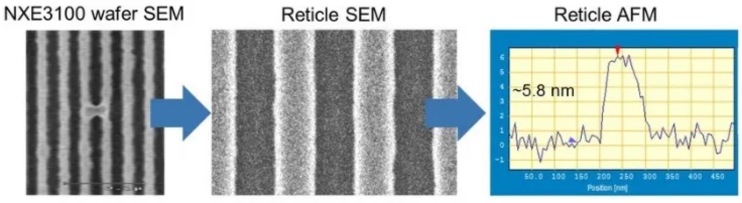
SEM and AFM inspection images of photomask defects of 27nm tech nodes
4. Electrostatics Impacts in Photomask Fabs
Electrostatic risks come form the repeated transfer handlings by automation robots and personnel, wet cleaning/drying processes, vacuum plasma etching process and the pellicle mounting process.
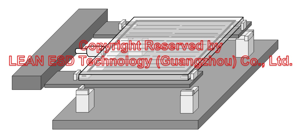
Electrostatics Impacts Photomask Model in Process Automations-Robot transferring
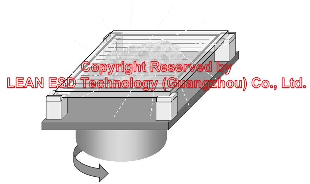
Electrostatics Impacts Photomask Model in Wet spinning process
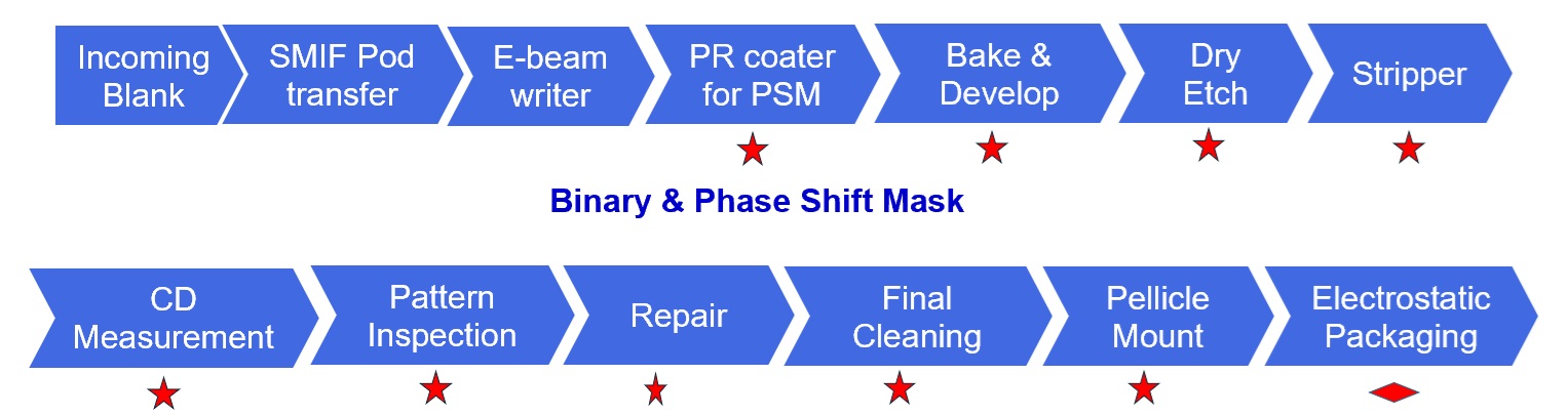
5. Electrostatics Protections Responsibilities of Photomasks
Photomask OEMs (Fab) take the responsibilities of photomask defect improvement in fabrication processes. And shall be responsible to screen out all the electrostatics induced defects (Hard failures by ESD and Soft failures by EFM) prior to shipment to users. The Effective Electrostatics Protective Packaging (Electromagnetic shielding) is a Must for all photomask products.
Photomask users (SEMI Wafer Fabs, FPD TFT Fabs, etc) shall the responsibilities to manage the electrostatics impacts on their photomasks throughout lithography transferring, regular CDU (Critical Dimension Uniformity) and particle inspections and the storage.
Photomask logistics suppliers shall make sure the protective packages of photomask products not be damaged throughout the journies.